SMT:
Well, you've designed your PCB and everything looks quite big on the computer screen, then the PCB arrives in the post... Next time I might rework the 0402 parts for 0603 or even 0805 so they can be hand placed!
This PCB will need mechanical help to place the components, especially as the TPS61200 boost converter is a 3 mm QFN package.
First for the solder application, there are three ways commonly used by people without access to specialised equipment. The 'blob and spread' as I call it, the syringe method and the most accurate, the stencil method.
The blob and spread method is basically put a small amount of solder paste on your PCB where your components are going to be placed. Spread the paste over the pads and place your components. Reflow the PCB. The solder will tend to pull onto the solder pads due to the way the fluxes in the paste control the solder melt, surface tension of the molten solder and the effect of the solder resist between the pads. Now you can see where you have solder bridges between you component pins and use a soldering iron and de-solder wick and/or scrapers to break the bridges.
The second method is to use a syringe to apply the paste in a more controlled fashion, reducing the tendency to form solder bridges. This can be effective for small components, but for the finest, the solder balls in the paste will be too big for the needle, so you will have to resort to larger needles and fix any bridging.
I'm going to use the third method, a solder stencil, as a syringe is not going to be an option with the smaller components.
You can buy a stencil from the PCB supplier, but they are quite expensive for small runs or prototyping. You can buy stencils from specialists on the Internet that use some form of plastic sheet rather than professional stainless steel sheet and CO2 lasers to cut them. These are much cheaper, but you will tend to see both buckling of the sheet and a limit to the size of aperture.
As I have access to a CO2 laser, I will produce a stencil.
First you need to export your PCB outline and cream layer from you PCB layout program. I'm using Eagle They produce a free version for amateur use, educational and professional versions, but there are OSS alternatives such as Free PCB, KiCAD and the Geda Project.
I print the layers to a postscript file and import that in to Corel 8, yes it still works even though it's 15 years old. If it didn't work, I'd use Inkscape or a similar package. When you import, import the files a curves, not text.
Select all the pads and lines and set there width to the smallest available. Now the boring part. The pads all need to be made smaller, for two reasons, the width of the laser beam and to account for the way the stencil material burns under the laser beam.
The laser cuts by vaporising the material in the path of the beam, as the material burns it tends to burn back or melt the substrate and the holes created tend to be larger. The pads needs selecting and scaling to 98%, unfortunately this can't be done in Corel by selecting all the objects, this would also scale the position of the pads in relation to the centre of the PCB. You need to select each pad individually, scale it to 98% and move on the the next. This will scale each pad but its position will remain constant as the scaling to done relative to the pads centre.
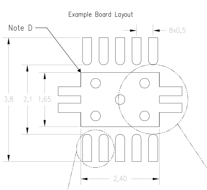
This scaling will reduce the RFM22B pads from 1.99 mm x 1.312 mm to 1.95 mm x 1.286 mm, a small but significant amount.
Now select all the pads and the PCB outline and group them together and save the file. Select the object, copy it and close the file.
Open the PCB Stencil Jig created by following the Laser cutting guide above. Create a new layer and paste the PCB from the copy buffer on to the new layer. Select the PCB outline on layer 1 of the Jig and note the X and Y position co-ordinates. Now select the new stencil object and enter the co-ordinates in the X and Y text boxes to move the PCB in to alignment with the Jig. Following the move, with the object still selected, right click and select un-group. This will separate the PCB outline from the pads, delete the outline and save the jig file.
If you want, you can create an outline for the stencil that is about 25 mm wider than the PCB outline and long enough to contain the three hexagonal registration holes needed to hole the stencil in place. If you don't do this, you can make the stencil the same size as the jig, both options are valid, the second just uses more material. Save the file again if you make the stencil outline.
"Stop... Laser Time!" © MC Hammer 1990
Laser cutters can use two methods to cut material, Vector [see Laser] or Raster.
Raster graphics is an image or bitmap, where the data structure representing the image is constructed from a grid of discrete pixels. In raster mode, a laser will fire and burn or vaporise a dot on the substrate, then move and fire again, building up a matrix of dots that remove the material leaving a hole in the substrate.
This method is much slower than vector, whereas vector would cut a line around a pad and the pad would fall out leaving the whole, the raster scans back and forth over the substrate vaporising all the material in the area defined as a pad. We have found the raster method to produce the best stencils and we tailor the run to burn part way through the substrate and run the jobs several times to make the cleanest stencil we can. Using this method, it is possible to produce a stencil for the fine chips like the 0.5 mm spaced QFN package of the regulator.
 |
.png) |
 |
The substrate that we use is not plastic film. The usual choices for amateur stencils cut by laser are Mylar [PET] or Kapton [Polyimide]. We don't.
Part two follows shortly.